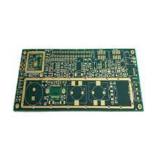
Fast Turn Prototype PCB Boards Made Quality
When a project calls for fast turn prototype PCB boards, you need to know what to expect in order to get your board delivered as efficiently as possible. This includes preparing the necessary files, design rules, specifications, and documentation. It also means setting the board up for success in terms of layer stackup, silkscreen clearances, and other details that impact fabrication costs and quality.
Whether your product is in the development stage or you are just readying a new release to market, having access to rapid prototyping is key. This is because it helps you to make changes to the product more quickly and easily. As a result, you can avoid costly mistakes and re-designs.
This is especially important for complex electronics, such as those used in electric vehicles and industrial applications. PCBs are the brains behind these high-tech systems, and it is crucial to ensure that the circuits work as intended. The best way to do this is through fast turn prototype pcb board, which allow you to test and refine your designs before production.
As the demand for electronic devices increases, many companies are embracing faster turnaround times to keep up with consumer demand. However, this can increase the risk of compromising on quality and other factors. This is why it is crucial to choose a fast-turn manufacturer that has the experience and expertise to deliver high-quality products.
How Fast Turn Prototype PCB Boards Are Made
The process of making a fast-turn prototype pcb board begins with a designer preparing the layout file and then uploading it to the online ordering system. The PCB manufacturer then checks the file for errors or omissions and outlines the assembly steps that need to be taken. The file is then sent to the production line, where the board is fabricated according to the specified specifications and quality assurance inspections are carried out at each stage of the process.
In addition, the manufacturer should provide a list of technical questions (TQs) within hours of receiving the file so that these can be resolved before production starts. This will prevent production delays and help to minimize the number of rejected boards during manufacturing.
Another factor that impacts cost is the size of the board, and this can be determined by the layers in the circuit board and the type of materials used. The minimum thickness is typically 1.57 mm. However, it is important to note that this thickness is a standard value chosen for historical reasons and may not be the most suitable for all situations.
The layer stackup in a fast-turn PCB prototype is crucial because it determines the maximum yield that can be reliably produced per panel. As such, it is worth considering this in the floorplanning process and adjusting the design to maximize the yield. It is also worthwhile to check with the manufacturer for any specific limitations in terms of maximum panel sizes. By doing so, you can save a significant amount of money by ensuring that the circuit board is designed to fit the manufacturer’s capabilities.